We have compiled a list of manufacturers, distributors, product information, reference prices, and rankings for Printed circuit board visual inspection equipment.
ipros is IPROS GMS IPROS One of the largest technical database sites in Japan that collects information on.

Printed circuit board visual inspection equipment - List of Manufacturers, Suppliers, Companies and Products

Printed circuit board visual inspection equipment Product List

1~3 item / All 3 items

Displayed results

Introduction to Printed Circuit Board Appearance Inspection Equipment (Contract Manufacturing)

Here is a list of specifications and equipment for the 3D appearance inspection device for printed circuit boards.

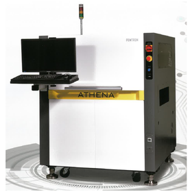
Hamamatsu Pulse handles everything from small-lot, multi-variety printed circuit board assembly to finished product assembly and packaging, and has established a system that allows for consistent product provision centered around production outsourcing. ◆ Line Name: 3D-AOI Visual Inspection Device: VT-S530 (Omron) ◆ Target Board Dimensions: 50(W)×50(L) to 680×510mm ◆ Inspection Targets: Missing parts/Position deviation/Polarity/Un-soldered/Shorts/Solder shape ◆ Target Component Height: Up to 50mm *For details, please download and view the materials.

  • Contract manufacturing

Added to bookmarks

Bookmarks list

Bookmark has been removed

Bookmarks list

You can't add any more bookmarks

By registering as a member, you can increase the number of bookmarks you can save and organize them with labels.

Free membership registration

3D inspection is possible! ~I've never seen a printed circuit board inspection device like this~

Compatible from bare boards to DIP and assembly boards! Inspection is possible in 3D, allowing for thorough verification of the surface irregularities of the inspection target.

The printed circuit board (raw substrate) surface inspection device "ATHENA" is a new product that enables three-dimensional appearance inspection. With cutting-edge 3D and AI technology, it has become possible to detect defects that were previously invisible. It can simultaneously inspect not only dents and scratches but also land processing defects, resist defects, and silk defects, significantly reducing the labor involved in the inspection process and contributing to cost reduction. It has been adopted by major semiconductor manufacturers and automotive manufacturers, and it is a product with high quality and precision. If you are interested, please feel free to contact us. 【Features】 ■ Spacious design and convenient maintenance ■ Simple assembly and setup ■ 3D formation of high-density components and components in narrow spaces ■ 3D formation identical to real images ■ Improved repeatability accuracy *For more details, please refer to the PDF document or feel free to contact us.

  • Other conveying machines
  • Substrate transport device (loader/unloader)

Added to bookmarks

Bookmarks list

Bookmark has been removed

Bookmarks list

You can't add any more bookmarks

By registering as a member, you can increase the number of bookmarks you can save and organize them with labels.

Free membership registration

For inquiries about microscope inspections with increased magnification, please consult Toyota Electronics.

Our employees, who are experts in printed circuit boards, will solve your company's problems!

Our company conducts inspection and processing of printed circuit boards. Using microscopes/magnifying glasses, we perform visual inspections of PWBs (printed circuit boards) for automotive, industrial, and semiconductor components, making pass/fail judgments based on customer specifications. We have also introduced automatic visual inspection equipment (AVI). The inspection environment is maintained at a cleanliness level of approximately 10,000, equipped with air cleaners and air showers. 【Features】 ■ We can accommodate inspections and sorting of small parts that require microscopes or magnifying glasses, not just circuit boards. ■ For tasks other than inspection, we have partner companies both domestically and internationally, allowing us to propose total support for printed circuit board design (domestic), manufacturing (domestic and international), assembly (domestic), etc. *For more details, please download the PDF or contact us.

  • Circuit Board Inspection Equipment

Added to bookmarks

Bookmarks list

Bookmark has been removed

Bookmarks list

You can't add any more bookmarks

By registering as a member, you can increase the number of bookmarks you can save and organize them with labels.

Free membership registration